
Modifier la traduction
mV Pressure Sensor Signal Conditioning Circuit Design

Pressure Sensor Signal Conditioning & Amplification Circuit Design
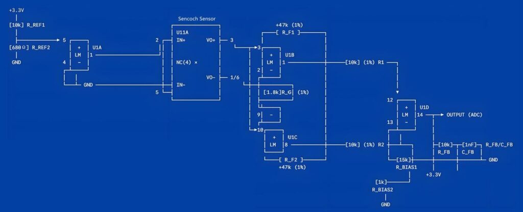
This document details a signal conditioning circuit designed for piezoresistive pressure sensors (such as the GZP160 series) featuring zero-point outputs from -5 mV to +10 mV and full-scale outputs from 60 mV to 100 mV. Operating on a single +3.3V supply, the architecture integrates a +0.206 V DC bias network to eliminate negative clipping at the low end and preserves a 13% engineering safety margin for ADC sampling.
1. Complete Schematic Diagram (Horizontal Layout)
=====================================================================================================
Excitation Buffer (U1A) ──► Sensor Unit (XGZP) ──► Stage 1: InAmp (U1B/U1C) ──► Stage 2: Bias Adder (U1D)           =====================================================================================================
2. Bill of Materials (BOM)
Designator | Value / Part Number | Tolerance / Forfait | Primary Function & Role |
U1 (U1A~U1D) | LMV324 / LM324 | SOIC-14 | Quad operational amplifier (Rail-to-Rail output recommended) |
R_F1, R_F2 | 47 kΩ | 0603, 1% | Feedback resistors for the 1st stage instrumentation amplifier |
R_G | 1.8 kΩ | 0603, 1% | Gain setting resistor (1st stage gain A_v1 ≈ 53.2x) |
R1, R2, R_FB | 10 kΩ | 0603, 1% | 2nd stage differential-to-single-ended network (Gain A_v2 = 1x) |
R_BIAS1 | 15 kΩ | 0603, 1% | Pull-up resistor for DC bias network (shifts offset to +0.206 V) |
R_BIAS2 | 1 kΩ | 0603, 1% | Pull-down resistor for DC bias network |
R_REF1 | 10 kΩ | 0603, 1% | Excitation divider pull-up resistor |
R_REF2 | 680 Oh | 0603, 1% | Excitation divider pull-down resistor (~0.21 V output) |
C_FB | 1 nF | 0603, NPO | First-order low-pass filter capacitor (Cutoff frequency ~15.9 kHz) |
C_DEC1, C_DEC2 | 100 nF / 10 µF | 0603 / 0805 | High-frequency and low-frequency power supply decoupling capacitors |
3. Key System Parameters & Calculations
- Total Circuit Gain: Approximately 2x
- DC Offset Bias: +0.206 V
- Input to Output Mapping Table:
- -5 mV Input (Negative extreme offset) ──► ~0.05 V Output (Kept safely within ADC linear range, no negative clipping).
- 0 mV Input (Nominal zero point) ──► ~0.206 V Output.
- +10 mV Input (Positive extreme offset) ──► ~0.74 V Output.
- +100 mV Input (Full-scale maximum) ──► ~2.87 V Output (Leaves a 13% headroom under +3.3V to prevent ADC saturation).
- MCU Compatibility: Fully compatible with 3.3V/5V microcontroller ADCs (par exemple., STM32, ESP32, Arduino).
※ If you need amplified circuit design proposal, please contact Sencoch.